


Laser Chip
BrandNew: Your Professional Laser Diode Manufacturer!
Extensive product line
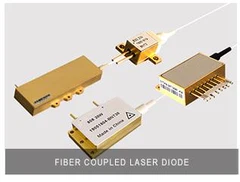
Founded in 2011, Professional Laser diode supplier, manufactures high-power diode lasers and systems in a wide range of output powers and wavelengths including laser chip, fiber coupled laser diode, single bar and high power diode laser array.
Quality Assurance
BrandNew pursues high quality, high efficiency, and high standard testing process to ensure that each product is tested at every level before shipment, and we strive to deliver perfect products to our customers, providing customers with a pleasant shopping experience and usage experience.
Customized Service
BrandNew designing and manufacturing a wide range of configurable and custom laser diode modules for machine vision, medical equipment, security, 3D printing, UV curing, and many other challenging applications.
24H Online Service
BrandNew Company offers 24-hour online support for advanced laser diode solutions. The BrandNew sales team has rich knowledge reserves and can help customers solve problems professionally.


What is Laser Chip?

Laser chip, also called unmounted diode laser bar, is single-emitter laser chip or single-bar laser chip, which are not mounted to a heat sink and lack any exterior packaging. Select from GaAs, InP, and GaSb semiconductor materials to get wavelength from 450 nm to 2 µm, which deliver exceptional reliability and performance.
A laser chip is a miniaturized chip that integrates lasers and other optoelectronic components. The core component of a laser chip is a semiconductor laser, which uses the recombination process of electrons and holes in semiconductor materials to generate lasers. Laser chips are smaller and lighter than traditional gas lasers or solid-state lasers, making them suitable for integration into various portable and embedded devices.
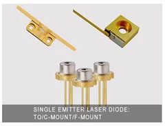
Single Emitter
Single Bar
VCSEL Chip
What are the existing products for Laser Diode Chip?
Single Emitter EEL Chip
| Wavelength | Item Number | Power | Emitter Width |
| 450nm | LC450SE5 | 5W | 45µm |
| 520nm | LC520SE1 | 1W | 100µm |
| 638nm | LC638SE500 | 500mW | 40µm |
| LC638SE1 | 1W | 110µm | |
| 660nm | LC660SE500 | 500mW | 40µm |
| LC660SE2 | 2W | 110µm | |
| 755nm | LC755SE8 | 8W | 350µm |
| 780nm | LC780SE2 | 2W | 100µm |
| LC780SE5 | 5W | 100µm | |
| 793nm | LC793SE10 | 10W | 200µm |
| 808nm | LC808SE1 | 1W | 50µm |
| LC808SE2 | 2W | 100µm | |
| LC808SE3 | 3W | 130µm,200µm | |
| LC808SE5 | 5W | 200µm | |
| LC808SE10 | 10W | 200µm | |
| LC808SE25 | 25W | 400µm | |
| 830nm | LC830SE2 | 2W | 47µm |
| 850nm | LC850SM500 | 500mW | 5µm |
| 880nm | LC880SE10 | 10W | 200um |
| LC880SE15 | 15W | 200um | |
| 905nm | LC905SE25 | 25W | 75µm |
| LC905SE50 | 50W | 135µm | |
| LC905SE75 | 75W | 200µm | |
| LC905SE100 | 100W | 300µm | |
| LC905SE200 | 200W | 300µm | |
| 915nm | LC915SE10 | 10W | 100µm |
| LC915SE15 | 15W | 190µm | |
| LC915SE20 | 20W | 190µm | |
| LC915SE30 | 30W | 280µm | |
| 940nm | LC940SE2 | 2W | 190µm |
| LC940SE12 | 12W | 95µm | |
| LC940SE20 | 20W | 190µm | |
| 976nm | LC976SM500 | 500mW | 5µm |
| LC976SM1500 | 1500mW | 5µm | |
| LC976SE12 | 12W | 95µm | |
| LC975SE15 | 15W | 190µm | |
| LC975SE20 | 20W | 190µm | |
| LC975SE25 | 25W | 230µm | |
| LC975SE30 | 30W | 280µm | |
| LC975SE35 | 35W | 300µm | |
| LC975SE45 | 45W | 330µm | |
| LC975SE70 | 70W | 330µm | |
| 1064nm | LC1064SM300 | 300mW | 5µm |
| LC1064SE8 | 8W | 95µm | |
| LC1064SE10 | 10W | 190µm | |
| 1470nm | LC1470SE3 | 3W | 100µm |
| LC1470SE5 | 5W | 190µm | |
| 1550nm | LC1550DFB100 | 100mW | 5µm |
| LC1550SE3 | 3W | 100µm | |
| LC1550SE5 | 5W | 190µm | |
| 1940nm | LC1940SE1 | 1W | 90µm |
Single Bar EEL Chip
| Wavelength | Item Number | Power | Number of Emitters | Emitter Width | Emitter Pitch | Cavity Length |
| 755nm | LC755SB50 | 50W | 19 | 150µm | 500µm | 1mm |
| LC755SB100 | 100W | 47 | 110µm | 200µm | 1.5mm | |
| 780nm | LC780SB60 | 60W | 47 | 100µm | 200µm | 1.5mm |
| LC780SB100 | 100W | 47 | 100µm | 200µm | 1.5mm | |
| 808nm | LC808SB50 | 50W | 19 | 150µm | 500µm | 1mm |
| LC808SB100 | 100W | 47 | 100µm | 200µm | 1.5mm | |
| LC808SB200 | 200W | 60 | 120µm | 160µm | 1mm | |
| LC808SB300 | 300W | 60 | 120µm | 160µm | 1.5mm | |
| LC808SB500 | 500W | 60 | 120µm | 160µm | 1.5mm | |
| 880nm | LC880SB50 | 50W | 19 | 150µm | 500µm | 1mm |
| 940nm | LC940SB100 | 100W | 19 | 150µm | 500µm | 2mm |
| LC940SB300 | 300W | 38 | 190µm | 250µm | 1.5mm | |
| LC940SB500 | 500W | 38 | 240µm | 280µm | 2mm | |
| LC940SB600 | 600W | 40 | 190µm | 250µm | 2mm | |
| LC940SB700 | 700W | 44 | 190µm | 230µm | 2.5mm | |
| LC940SB1000 | 1000W | 37 | 190µm | 250µm | 4mm | |
| 976nm | LC976SB40 | 40W | 5 | 100µm | 1000µm | 4mm |
| LC976SB100 | 100W | 47 | 100µm | 200µm | 1.5mm | |
| LC976SB200 | 200W | 47 | 100µm | 200µm | 4mm | |
| 1064nm | LC1064SB50 | 50W | 19 | 150µm | 500µm | 1.5mm |
| LC1064SB100 | 100W | 49 | 100µm | 200µm | 1.5mm | |
| 1470nm | LC1470SB25 | 25W | 19 | 100µm | 500µm | 2mm |
| 1550nm | LC1550SB25 | 25W | 19 | 100µm | 500µm | 2mm |
What is the difference between single emitter laser chip and single bar laser chip?

The main difference between single emitter laser chip and single bar laser chip is their structure and application. Single emitter laser chip usually refer to a single laser chip, while single bar laser chip are strip-shaped structures composed of multiple laser chips.
Single emitter laser chip is composed of a single laser chip and usually have a smaller size and lower power output. They are usually used in applications that require precise control of the beam, such as fiber-optic communications and laser pointers. The characteristics of single emitter laser chip are their high beam quality and are suitable for applications that require high directivity and high brightness.
Single bar laser chip are strip-shaped structures composed of multiple laser chips and usually have a larger size and higher power output. Single bar laser chip are suitable for applications that require high power output, such as material processing, medical equipment, and scientific research instruments. The characteristics of single bar laser chip are their high output power and are suitable for applications that require large-area irradiation or high energy.
In terms of technical details and applications, single emitter laser chip and single bar laser chip also differ in preparation methods and material selection. Single emitter laser chip are usually prepared using metal organic chemical vapor deposition technology and have high beam quality and efficiency. The single bar laser chip avoids side lasing through the design of epitaxial layer and isolation groove, and improves the reliability and durability of the device.
Can unmounted laser bars be cut into single emitter laser chips?
Unmounted laser bars can be cut into single emitter laser chips, including the following steps:
Scribing: On each unmounted laser bar to be cleaved, scribing is performed between two adjacent chips.
Film expansion: The adhesive film with the laser bar attached is transferred to the film expansion machine for the first film expansion. After the film expansion is completed, the adhesive film is in the first expansion state and remains in this state.
Splitting: The adhesive film in the first expansion state is transferred to the splitting machine, and the laser bar is split along the scribing line to separate the chips on the laser bar from each other. By expanding the adhesive film attached to the laser bar before splitting, prestress is provided to the chips on both sides of the scribing line, so that the chips can be naturally separated cleanly along the scribing direction during splitting, avoiding the chips from colliding with each other during splitting and being damaged.
The key to this method is to provide prestress by film expansion to ensure that the chips can be naturally separated along the scribing direction during splitting, thereby improving the yield and quality of the chips.
How does the pitch or spacing between emitters on the unmounted laser bar impact performance?

The spacing between the emitters of the unmounted laser bar has a significant impact on performance. Uniform emitter spacing can ensure better heat dissipation effect of the unmounted laser bar, thus improving the life and stability of the unmounted laser bar.
The distance between the emitters of the unmounted laser bar will affect the heat dissipation effect. If the spacing of the emitters is uneven, it may cause the temperature of some emitters to be too high, thus affecting the performance and life of the laser. By adjusting the width of each emitter of the bar, the heat dissipation of the entire bar can be made more uniform, and the temperature of the middle emitter can be avoided to be significantly higher than the temperature of the edge emitter, thereby reducing the problems of wavelength shift and pulse width reduction.
The spacing between the emitters also affects the brightness of the unmounted laser bar. If the distance between the emitters is too large, it may cause uneven brightness and affect the display effect. The appropriate spacing between emitters can ensure the display effect and performance of the unmounted laser bar in different application scenarios.
Are there any requirements for the heat sink used in packaging eel laser chips?
There are multiple requirements for heat sinks used in packaging laser chips, mainly including thermal conductivity, thermal expansion coefficient matching, thermal stress release capability and surface treatment.
First, thermal conductivity is one of the important parameters of heat sink materials. Laser chips generate a lot of heat during operation. If the heat cannot be dissipated in time, it will affect the performance and life of the laser. Therefore, the heat sink material needs to have a high thermal conductivity in order to effectively conduct the heat away. Common heat sink materials such as aluminum nitride, silicon carbide, diamond, etc. have high thermal conductivity.
Second, thermal expansion coefficient matching is also very important. The thermal expansion coefficients of laser chips and heat sink materials need to match to reduce stress caused by temperature changes and prevent cracks or deformation between materials. For example, the thermal expansion coefficient of aluminum nitride is 4.6×10^-6/K, which is close to the thermal expansion coefficient of laser chips, so it is often used as a transition heat sink material.
In addition, thermal stress release capability is also a key factor. The heat generated by the laser during operation will cause thermal stress between the chip and the heat sink. If the heat sink material cannot effectively release these stresses, it may cause the laser performance to degrade or fail. Therefore, the heat sink material needs to have good thermal stress release capabilities.
Finally, the surface treatment also affects the performance of the heat sink. The surface treatment of the heat sink material needs to meet certain appearance and physical and chemical test requirements to ensure its reliability and durability in practical applications.
In summary, the heat sink used for packaged laser chips needs to have high thermal conductivity, match the chip's thermal expansion coefficient, good thermal stress release capabilities and appropriate surface treatment to ensure the stability and long-term reliability of the laser.
How to package unmounted laser chip bars?

The core steps of packaging unmounted laser chip bars include: selecting appropriate packaging materials, designing the packaging structure, performing welding and bonding, and optimizing thermal management.
First of all, choosing the appropriate packaging material is the key to ensuring the performance of the unmounted laser chip bar. For example, gold-tin hard solder can be used to package high-power gallium nitride (GaN) blue semiconductor laser bars, and a copper-tungsten transition heat sink can be used as a buffer layer to suppress packaging residual stress. In addition, the InGaAs/AlGaAs epitaxial material system can also be used to design high-power tapered semiconductor laser bar arrays.
Secondly, a properly designed packaging structure is crucial to improving the performance of unmounted laser chip bars. For example, the package structure can be built using components such as microchannel heat sinks, insulating films, and copper tapes to achieve good thermal management and current distribution.
Next comes the soldering and bonding process. A high-precision placement machine is used to eutectic-bond the chip to the copper-tungsten transition heat sink, and the welding temperature, pressure and time are strictly controlled to ensure welding quality. Experiments show that appropriate welding parameters can significantly reduce thermal resistance and threshold current, thereby improving output optical power and photoelectric conversion efficiency.
Finally, optimizing thermal management is an important measure to ensure long-term stable operation of unmounted laser chip bars. By rationally designing the heat sink structure and selecting appropriate materials, the thermal resistance can be effectively reduced, the heat dissipation efficiency can be improved, and the service life of the unmounted laser chip bars can be extended.
Why do we need to package unmounted laser bar in a clean room?
1. Prevent contamination: The unmounted laser bar needs to be packaged in a dust-free and sterile environment to prevent the intrusion of particles and microorganisms. These contaminants may affect the performance and life of the unmounted laser bar, and even cause packaging failure.
2. Improve packaging quality: Environmental control in the clean room can ensure that the temperature, humidity and air flow during the packaging process are in the best state, thereby improving the packaging quality and consistency. This helps to reduce packaging defects and improve the qualified rate of products.
3. Extend service life: Packaging in a clean environment can reduce the damage to the unmounted laser bar by external factors, thereby extending its service life. The clean room reduces the pollution problems that may be encountered during the packaging process by strictly controlling the environmental conditions, and protects the stability and reliability of the unmounted laser bar.
4. Improve production efficiency: The efficient filtration system and strictly controlled environmental conditions of the clean room can reduce production interruptions and rework caused by pollution, thereby improving overall production efficiency. In addition, the clean room can also ensure the continuity and stability of the production process, further improving production efficiency.
What is the difference between EEL chip and VCSEL chip?

Structural differences:
EEL (Edge Emitting Laser): EEL uses radiation emission along the axis direction, that is, the light is emitted along the plane direction of the device, usually with a cylindrical structure, and the light emits a laser beam from the side.
VCSEL (Vertical Cavity Surface Emitting Laser): The structure of VCSEL is vertical, that is, the light is perpendicular to the device, and the light is mainly emitted from the top, forming a circular spot.
Emission mode:
EEL: The laser beam is emitted from the side through a cylindrical structure.
VCSEL: Surface emitting laser, the light is mainly emitted from the top.
Spot shape:
EEL: The emitted spot is elliptical.
VCSEL: The emitted spot is circular.
Performance differences:
EEL: It has higher output power and energy of a single laser, suitable for applications with high energy requirements.
VCSEL: It has high internal quantum efficiency and better thermal stability, and can achieve high speed, low power consumption and a wide temperature range.
Application areas:
EEL: It is mostly used for high-speed communications, such as fiber-optic communications, laser printing, optical discs, and optical measurement and detection.
VCSEL: It is commonly used in data center optical interconnection, lidar, facial recognition, 3D scanning and other applications.
In summary, EEL and VCSEL have significant differences in structure, emission mode, spot shape, performance, and application areas. Users can choose the appropriate laser chip according to specific needs.
How does the EEL Edge Emitting Laser Chip work?
The work of the EEL Edge Emitting Laser chip mainly includes the following steps:
1. Carrier injection: By applying a forward bias, electrons are injected from the N-type region into the active layer, and holes are injected from the P-type region into the active layer. In the active layer, electrons and holes recombine to generate photons. This process is similar to a light-emitting diode (LED), but EEL is to achieve lasers instead of ordinary light.
2. Stimulated radiation and light amplification: Photons generated in the active layer interact with other excited electrons, causing these electrons to transition to a low energy state and emit more photons with the same phase, frequency and direction as the initial photons. This is stimulated radiation. When photons reflect back and forth between these mirrors, more stimulated radiation photons are generated in the active layer, forming a light amplification mechanism in the resonant cavity.
3. Resonant cavity and light amplification: Since the active layer of the EEL is embedded between two parallel mirrors (end faces), these mirrors will reflect some photons back to the active layer. When photons reflect back and forth between the two mirrors, more stimulated radiation photons are generated in the active layer. This repeated light amplification process forms the light amplification mechanism in the resonant cavity.
4. Laser output: When the number of photons in the resonant cavity reaches a certain threshold, some photons will be emitted through the end face with lower reflectivity to form laser output. The direction of the laser beam of EEL is parallel to the surface of the chip, so it is called an edge-emitting laser.
What are the cooling methods for diode laser chips?

Four cooling Methods
Natural convection heat sink cooling: This method uses materials with high thermal conductivity to remove the generated heat and dissipate the heat by natural convection. In addition, fins can also help dissipate heat and improve the heat transfer rate of the cooling system.
Thermal conductivity materials: Use materials with high thermal conductivity to reduce the temperature of the laser. These materials can effectively conduct heat away, thereby maintaining the stable operation of the laser.
Liquid cooling system: The liquid cooling system absorbs and removes heat by circulating liquid, and has a high thermal conductivity efficiency. This method is suitable for high-power lasers and can effectively reduce the temperature of the laser to ensure its long-term stable operation.
Air cooling system: The laser is cooled by a fan or airflow, which is suitable for medium-power lasers. The air cooling system has a simple structure and is easy to maintain, but the heat dissipation effect may not be as good as the liquid cooling system.
What we can offer in Laser Chip?
Based on industry-leading semiconductor technology, BrandNew provides a wide range of laser chip options. Some of these options include wavelengths ranging from 450nm up to 2100nm, single-emitter laser chip with up to 20W output power and single-bar laser chip with up to 600W output power, and continuous wave (CW) and quasi-continuous wave (QCW) options. Laser chip and bar are available in various fill factors, stripe widths, bar widths, and cavity lengths, and customized options can be developed to meet your unique requirements.
Advantages of our Laser Chip
Laser chips are produced under the strictest quality controls. We work only with state-of-the-art epitaxy, processing, and facet coating technology. Standard soldering methods are used for assembling laser chip. The material supports both soft solder (indium) and hard solder (gold/tin). The standard configuration of the laser chip is an emitter structure separated on the p-side. On request, laser chips are available with continuous p-side metallization and adapted facet coatings, using low AR coatings for the assembly of external resonators.
Features of Laser Chip
High quality
We strictly monitor the production of our laser chip products in clearly defined processes. Unique state-of-the-art epitaxial technology for highest reliability and lifetime.
01
Powerful
High, reliable output power and ideal beam characteristics.
02
Economical
High efficiency and characterized by a long service life.
03
Production Capacity
We can offer high volume production capacity over a wide range of powers and wavelengths.
04
Precautions For The Use Of Laser Diodes
The laser light emitted from this Device is invisible and will harmful to the human eye. Avoid looking directly into the fiber output or into the collimated beam along its optical axis when the device is in operation. Proper laser safety eyewear must be worn during operation.
Absolute Maximum Ratings may be applied to the Device for short period of time only. Exposure to maximum ratings for extended period of time or exposure above one or more max ratings may cause damage or affect the reliability of the Device.
Operating the product outside of its maximum ratings may cause device failure or a safety hazard. Power supplies used with the device must be employed such that the maximum peak optical power cannot be exceeded. A proper heat sink for the Device on thermal radiator is required, sufficient heat dissipation and thermal conductance to the heat sink must be ensured.
The Device is an Open-Heat sink Diode Laser; it may be operated in clean room atmosphere or dust-protected housing only. Operating temperature and relative humidity must be controlled to avoid water condensation on the laser facets. Any contamination or contact of the laser facet must be avoided.
ESD PROTECTION – Electrostatic discharge is the primary cause of unexpected product failure. Take extreme precaution to prevent ESD. Use wrist straps, grounded work surfaces and rigorous antistatic techniques when handling the product.
Order process

Our Certificate

Our Clean Room


Hangzhou Brandnew Technology Co., Ltd. is one of the leading laser chip manufacturers and suppliers in China, has a professional factory which manufacturers high quality laser chip and sells at competitive price. Welcome to wholesale our products made in China.