



Why Choose Between VCSEL Die, SMD, and TO-Can Packages for Your Optical Integration?
Selecting the correct packaging form for vertical-cavity surface-emitting lasers (VCSELs) is a critical decision that influences manufacturing efficiency, thermal dissipation, and overall system cost. As design engineers integrate high-power VCSEL arrays into consumer electronics, automotive LiDAR, and industrial sensing platforms, understanding the performance profiles, assembly requirements, and economic curves of bare die, surface-mount device (SMD), and TO-Can packages is essential for successful commercialization.
Bare VCSEL die is the lowest-cost option if you have die bonders, wire bonders and cleanroom capability. SMD packages such as 2121 and 4040 reflow directly onto PCBs and suit automated consumer and automotive lines. TO-Can packages are plug-and-play for R&D, industrial sensing and low volume. Volume production favors SMD, prototyping favors TO, and vertically integrated customers favor die.
Physical and Process Differences Across Packaging Forms
Each VCSEL packaging format requires distinct handling, assembly methods, and manufacturing environments during system integration.
Bare Die Configuration:
Unencapsulated semiconductor chips that require specialized eutectic or silver-epoxy die attachment followed by wire bonding directly to the circuit substrate.
Surface-Mount Device Packaging:
Molded or ceramic-based packages (such as 2121 and 4040 form factors) that integrate protective encapsulation and electrical contact pads compatible with standard surface-mount technology (SMT) reflow soldering lines.
TO-Can Metal Encapsulation:
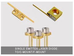
A robust metal can housing featuring an integrated optical window or flat lens, providing hermetic sealing and physical protection for the emitting semiconductor chip.

Thermal Path Management and Power Density
Thermal resistance and heat dissipation capabilities vary significantly across packaging designs, particularly as optical output power scales upward.
SMD Thermal Pathways
Thermal resistance in SMD packages depends heavily on printed circuit board (PCB) layout design, copper trace thickness, and dedicated thermal pad integration beneath the package base.
TO-Can Fixed Conduction
TO-Can packages feature a standardized metal header thermal path well-suited for medium-power VCSEL arrays and continuous-wave operation.
High-Power Multi-Junction Demands
Advanced multi-junction VCSEL architectures concentrate higher optical power within compact emission areas, placing strict thermal management requirements on the underlying package and heat sink structure.
Volume Readiness and Manufacturing Scalability
High-Volume SMD Integration
Capital Requirements for Bare Die
Prototyping Suitability for TO-Can
Cost Curve Comparison and Economic Trade-Offs
The economic viability of each package type shifts depending on total production volume and in-house manufacturing capabilities.
Low-Volume Production:
TO-Can packages deliver the lowest total cost by eliminating specialized tooling and surface-mount setup expenses.
High-Volume Production:
SMD packages achieve the lowest per-unit cost through automated pick-and-place reflow soldering.
Very High Volume Integration:
Vertically integrated manufacturers with established packaging lines achieve the lowest long-term unit cost by utilizing bare VCSEL die.
Our address
RM1705, Building 2, Aoqiang Mansion, No. 6 Xiyuan 5th Rd
Phone Number
86 181 5840 0345
wp@brandnew-china.com