


The emergence of high-power semiconductor lasers can be traced back to the 1960s. They were initially used in the fields of communications and sensing, and their power levels were relatively low. It was not until the 1980s and 1990s that the output power of high-power semiconductor lasers gradually increased, and they showed potential for application in more fields. After entering the 21st century, high-power semiconductor lasers continued to innovate in technology. At present, high-power semiconductor lasers have the characteristics of high output power, excellent thermal management capabilities, and excellent reliability. They are widely used in the fields of industrial material processing, solid-state laser pumping, and scientific research.
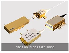
Solid-state laser pumping is one of the important application directions of high-power semiconductor lasers. By combining high-power semiconductor lasers with solid laser media, powerful and controllable laser output can be achieved. In recent years, with the continuous development of the field of solid-state lasers, more and more new applications have gradually emerged. For example, using Nd: YAG as a laser crystal, it is possible to achieve the output of high-power 1064nm laser (CW or QCW mode), which is ultimately applied to advanced manufacturing fields such as precision material processing, hard material cutting (such as diamond cutting, frequency doubling 532nm), surface treatment, and pan-semiconductor processes. By using Ho/Tm/Er: YAG crystals or ceramics, "eye-safe" lasers in the wavelength range of 1.4 to 3 μm can be obtained, which have very broad application prospects in the fields of laser radar ranging, communications, 3D imaging or gated imaging. Among them, lasers in the 2μm wavelength range can also be used for local heating and precise cutting of various polymers (such as polymer plastics), interface welding, etc. In addition, water molecules also have a very high light absorption rate near 2μm, so lasers in this wavelength range also have very important applications in the medical field (such as tissue cutting, hemostasis, and stone crushing in urological surgery).
With the improvement of semiconductor chip technology and the continuous expansion of downstream applications, high-power semiconductor lasers used for solid-state laser pumping are rapidly developing in the direction of miniaturization. Miniaturization, as an important development trend, involves technical innovation and optimization in many aspects. Horizontal Array Diode Laser from Brandew relies on core technologies such as eutectic bonding, interface materials and surface engineering, and thermal management to achieve the advancement of integrated technology, the improvement of design efficiency, the upgrade of thermal management capabilities, and the improvement of product reliability and life.


Horizontal Array Diode Laser adopts compact structure design, advanced materials, and industry-leading eutectic bonding process, which reduces the thermal resistance of laser stack while ensuring product reliability. It is very suitable for solid laser pumping applications. Customers can design and manufacture smaller products under the same output conditions, or achieve higher power output under similar sizes. This advantage not only facilitates customers to integrate products and systems, but also further helps customers reduce costs, providing more miniaturized and efficient photonic application solutions for many mid- and downstream application fields.
Through the optimized design of the conduction structure, the heat generated by the chip is more efficiently transferred from the heat sink to the cooling water channel, achieving more effective heat exchange, ensuring that the same output power can be maintained in a more compact size, while also extending the product life.

Features of Horizontal Array Diode Laser
The features and benefits of Horizontal Array Diode Laser have set it apart from other diode lasers available in the market. Here are some of the notable features of Horizontal Array Diode Laser:
1. High-Power Output: Horizontal Array Diode Laser can produce an output of up to 10 kW, making it one of the most powerful laser sources available in the market.
2. Reliability: Horizontal Array Diode Laser is highly reliable and can withstand harsh environmental conditions, such as high temperatures and vibrations. It also has a long lifespan, which makes it a cost-effective solution for industrial applications.
3. Compact Size: Horizontal Array Diode Laser's compact size allows it to be easily integrated into existing industrial processes, making it a practical solution for various industrial applications.

Applications of Horizontal Array Diode Laser
Horizontal Array Diode Laser is an ideal solution for high-power laser applications in the industrial sector. Some of the common applications of Horizontal Array Diode Laser include:
1. Laser Cutting: Horizontal Array Diode Laser can be used for cutting various metals and non-metals, including aluminum, copper, stainless steel, and carbon steel.
2. Welding: Horizontal Array Diode Laser can be used for welding applications, such as spot welding, seam welding, and butt welding, in the automotive, aerospace, and shipbuilding industries.
3. Thermal Processing: Horizontal Array Diode Laser can produce a high-intensity light beam, which can be utilized for processing various materials, such as plastics, ceramics, and composites.
4. Medical Applications: Horizontal Array Diode Laser can also be used in the medical field, such as for surgical procedures, dental treatments, and dermatological treatments.
The product has good scalability and can flexibly customize the number of bars and output power according to customer needs. It can also be combined and matched according to customer application scenarios, and is widely applicable to various application fields.

Since its establishment, Brandnew has always focused on the research and development of basic components and related application products of photonic technology, and actively expanded innovative application fields. The company independently develops core technologies and products in the field of high-power semiconductor lasers and laser optics, and has an experienced technical R&D team. It has now formed nine core technologies: eutectic bonding technology, thermal management technology, thermal stress control technology, interface materials and surface engineering, test analysis and diagnosis technology, line spot shaping technology, beam conversion technology, light field homogenization technology and wafer-level synchronous structured laser optical manufacturing technology. The product has been iteratively upgraded on the basis of the previous generation of products, and its key indicators such as miniaturization, thermal management capabilities, and reliability have reached the domestic leading level. Brandnew makes full use of core technologies and successfully developed a series of high-power, high-reliability conduction-cooled stacked array products, and continues to explore and innovate, committed to providing customers with more flexible and efficient customized solutions.
Brandnew insists on technological innovation, excellent manufacturing and rapid response, and strives to become a global trusted photonic application solution provider.
Our address
B-1508 Ruiding Mansion,No.200 Zhenhua Rd,Xihu District 310030 Hangzhou China
Phone Number
0086-571-8898-7800
info@brandnew-china.com
