


With the continuous improvement of laser application requirements, the requirements for semiconductor lasers are also getting higher and higher, which are mainly reflected in the following aspects:
Improve output power, develop high-power two-dimensional or three-dimensional arrays to meet the power demand in industrial processing and other fields; improve electro-optical conversion efficiency, achieve miniaturization and high efficiency of laser systems, reduce heat dissipation pressure, and reduce costs; improve Beam quality; improve reliability, that is, it can be used freely in high peak power and extremely harsh environments, such as the use of space vehicles in environments with large radiation and large temperature differences.
Key Technologies of High Power Semiconductor Lasers
Structural Design Optimization
The development of high-power semiconductor lasers is closely related to the research and design of epitaxy and chip structures. Structural design is the basis of high-power semiconductor laser devices. The three basic principles of semiconductor lasers are: electrical injection and confinement, electro-optical conversion, optical confinement and output, respectively corresponding to the design of electrical injection, quantum well design, and optical field design of waveguide structures. The structural research and improvement of semiconductor lasers is based on the continuous optimization of these three aspects, the development of asymmetric wide waveguide structures, the optimization of quantum wells, quantum wires, quantum dots and photonic crystal structures, which promotes the continuous improvement of the level of laser technology. The output power and electro-optical conversion efficiency are getting higher and higher, the beam quality is getting better and better, and the reliability is getting higher and higher.
High-quality epitaxial material growth technology
Semiconductor laser epitaxial material growth technology is the core of semiconductor laser development. High-quality epitaxial material growth process, extremely low surface defect density and internal defect density are the prerequisites and guarantees to achieve high peak power output. In addition, impurities also play an important role in semiconductor materials. It can be said that there is no high-performance quantum well laser without precise semiconductor epitaxy doping process. Mainly through the optimization of the doping curve, the overlap between the optical field and the heavily doped region is reduced, thereby reducing the absorption loss of free carriers and improving the conversion efficiency of the device.
Cavity surface treatment technology
The application of high-power semiconductor lasers usually requires high laser output power and good reliability. The main bottleneck restricting the output power of semiconductor lasers is the optical catastrophe damage (COMD) caused by the degradation of the cavity surface under high power density.
In the cavity surface area of semiconductor lasers, there are a large number of defects due to cleavage, oxidation and other reasons, and these defects become light absorption centers and non-radiative recombination centers. The heat generated by light absorption increases the temperature of the cavity surface, and the increase in temperature causes the band gap to decrease, so a potential gradient is formed between the cavity surface area and the inner area of the laser, which guides the injection of carriers into the cavity surface area, which is more important The main point is that the interband light absorption is enhanced after the band gap is reduced, both of which will increase the carrier concentration in the cavity surface area, enhance the non-radiative recombination, and further increase the cavity surface temperature. On the other hand, the larger current injection of high-power semiconductor lasers also enhances the non-radiative recombination of the cavity surface. It is the positive feedback process of light absorption, non-radiative recombination, temperature increase and band gap reduction that causes the temperature of the cavity surface to increase rapidly, and finally the cavity surface burns out, that is, COMD occurs.
The root of the cavity surface problem is the existence of cavity surface defects, including contamination, oxidation, material defects, etc. of the cavity surface. These cavity surface defects first affect the consistency of COMD, and secondly lead to the degradation of the device and affect the long-term stability. Generally, various cavity surface passivation and coating techniques can be used to reduce or eliminate the defects and oxidation of the cavity surface, reduce the light absorption of the cavity surface, and improve the COMD value of the cavity surface, thereby achieving high peak power output.
Integrated Packaging Technology
The cooling and packaging of laser chips are an important part of manufacturing high-power semiconductor lasers, and laser beam shaping and laser integration technology are the main ways to obtain kilowatt and 10,000-watt lasers. Due to the high output power and small light-emitting area of high-power semiconductor lasers, the heat density generated during operation is very high, which puts forward higher requirements on the packaging structure and process. The key technology research of high-power semiconductor laser packaging is to start from the aspects of heat, packaging materials, and stress, to solve the packaging design of thermal management and thermal stress, and to achieve a technological breakthrough in the development of direct semiconductor lasers to high power, high brightness, and high reliability.
Applications of semiconductor lasers
The field of direct application of semiconductor lasers has been widely expanded. In addition to being used as a pump source for solid-state lasers and fiber lasers, it is also directly used in many fields such as optical communication, industrial processing, medical beauty, and lighting monitoring. In recent years, the new applications of semiconductor lasers in 3D sensing, lidar, laser display and other fields have attracted great attention.
Communications and Optical Storage
The field of optical communication is still the largest market for semiconductor laser applications, and optical fiber communication has become the mainstream of contemporary communication technology. It is also an ideal light source for optical parallel processing systems and can be used in optical computers and optical neural networks. At present, the main applications in the field of optical communication are 1.3 μm and 1.55 μm InGaAsP/InP semiconductor lasers. The red laser and blue laser, which are mainly used in optical information and storage, can realize high-density information storage and processing.
pump light source
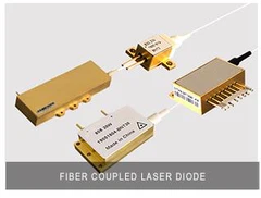
Semiconductor laser-pumped solid-state lasers and fiber lasers are the most widely used fields of high-power semiconductor lasers. As a pumping source, semiconductor lasers have the irreplaceable advantages of other light sources, and fiber lasers have become the most influential pumping market in the past five years. The pump source is divided into two categories: single-chip coupled fiber output and bar coupled fiber. Commonly used is 105 μm/NA0.22 fiber with continuous output of 30-120 W; 200 μm/NA0.22 fiber with continuous output of 50-300 W, with wavelengths covering 808-976 nm.

Laser Display and Medical
Laser display has huge market potential due to its advantages of large color gamut, high brightness, long life, and easy realization of large-screen display. In order to obtain a better visual experience, the shorter the wavelength of the red laser used for laser display, the better visual experience can be obtained. For example, the sensitivity coefficient of the human eye at 640 nm is 3 times that of 660 nm. However, for AlGaInP red semiconductor lasers, the shorter the wavelength, the higher the band gap of the active region material, and the carriers are more likely to overflow from the active region into the confinement layer, reducing the efficiency and reliability of the laser. Considering various factors, the wavelength of the red laser for laser display is generally 640 nm. In the field of laser medical treatment, the use of 650-680 nm red lasers is also becoming more and more eye-catching, and has been well used in physical therapy, cell detection, photodynamic therapy, etc.

industrial processing
The field of material processing is currently the second largest field of laser application, and it is also the fastest growing field recently, thanks to the rapid development of fiber laser technology. Laser processing is based on the photothermal effect processing of various materials. Under different laser power densities, the surface area of the material undergoes changes such as temperature rise, melting, gasification, and photoplasma. According to the degree of surface change, annealing and cladding are formed. , welding, cutting, drilling and other different applications.

lighting monitoring
With the enhancement of people's awareness of safety precautions, the requirements for surveillance cameras are getting higher and higher, especially in special occasions such as border/coastal defense, forest fire prevention, and railway traffic. Laser monitoring has the advantages of long detection distance, high reliability, low power consumption, and high definition, and has developed rapidly in long-distance monitoring applications. Semiconductor lasers represented by 940 nm have been widely used in high-speed rail, highway, forest fire prevention, border and coastal defense and other fields.
With the continuous advancement of technology, semiconductor lasers themselves have great room for expansion in terms of power, wavelength, and working methods, and further promote the development of emerging industries such as laser display, laser intelligent recognition, virtual reality, precision machining, and medical testing. With the rise, semiconductor lasers, as core components, have entered thousands of households, and are playing an increasingly important role in various fields of national economy and people's livelihood.
Welcome contact us for more details:
Whatsapp/Skype/Wechat: 0086 181 5840 0345
Email: info@brandnew-china.com