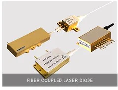
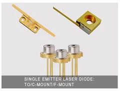
For a laser chip with a single output optical power of more than 500mW, it is already a high-power laser chip. The conversion efficiency varies according to the material. For example, the current high power of red light can reach 50%, and the remaining electrical energy is converted into heat energy.
For low-power LDs, such as the mW level used in optical communications, cavity surface catastrophe is generally rarely considered. High-power laser chips are prone to cavity surface catastrophe Catastrophic optical damage, COD. Optical catastrophic damage, also known as catastrophic optical mirror damage (COMD), is a failure mode of high-power lasers.
Usually we think that COD is caused by the semiconductor PN junction being overloaded due to exceeding the power density and absorbing too much light energy generated by the gain, which eventually leads to melting and recrystallization of the cavity surface area, and the affected area will produce a large number of lattice defects, which will destroy the performance of the device. When the affected area is large enough, we will call the cavity surface blackening, cracks, grooves and other phenomena observed under an optical microscope as "external COD mechanism".
Improving the red light chip's ability to resist COD (catastrophic optical mirror damage) can be achieved through a variety of methods, mainly including material selection, non-absorption window technology and chip design optimization.
Material selection:
The use of high-quality materials is the basis for improving COD resistance. For example, AlGaInP material shows good performance in the red spectrum and can be used to prepare high-efficiency red LEDs.
In Micro LED chips, the use of indium gallium nitride (InGaN) material, combined with V-shaped pit technology, can effectively alleviate the segregation of high In components, thus improving the overall performance of the chip.
Non-absorptive window technology:
Non-absorptive window technology is an effective method that can significantly reduce the light absorption of laser chips, thereby suppressing the generation of COD. For example, using the technology of Zn diffusion to form a non-absorbing window, a high-power 660nm semiconductor laser can be prepared, whose end-face light absorption is reduced, helping to suppress COD.

Chip design optimization:
During the chip design stage, the COD resistance can be improved by optimizing the structure and parameters. For example, by controlling the localization of carriers, the impact of surface non-radiative recombination on internal quantum efficiency can be greatly reduced, thereby improving the overall performance of the chip.
In the material epitaxy stage, optimization can also be performed to ensure the uniformity and stability of the material, thereby improving the COD resistance of the chip.
Other technical means:
Improving the conversion efficiency of laser chips is also an important direction. For a single laser chip with an output optical power of more than 500mW, the conversion efficiency can reach 50%, and the remaining electrical energy is converted into heat energy, which helps to reduce the temperature of the chip and thus improve its COD resistance.

In summary, by comprehensively using high-quality materials, non-absorption window technology, chip design optimization and other related technical means, the COD resistance of red light chips can be effectively improved, thereby improving their overall performance and reliability.
Once COD occurs, the chip will be irreversibly damaged, generally with a drop in optical power of more than 50%, or even no light. How to improve the chip's ability to withstand COD? We can make efforts in the material epitaxy stage, chip design stage, chip process stage, and chip end face cavity surface treatment.
Several options to improve chip resistance to COD:
1Strain quantum well technology
As the most widely used active region of semiconductor lasers, quantum wells exhibit quantized sub-band and step state densities inside, which will greatly improve the threshold current density and temperature stability of the laser; by changing the potential well width and barrier height, It can change the quantized energy interval and realize the tunable characteristics of the laser. Compared with the traditional double heterojunction semiconductor laser, it can effectively reduce the threshold current of the laser and improve the quantum efficiency and differential gain. The introduction of strain into the quantum well will significantly change its own energy band structure. By adjusting the positions of the heavy and light hole bands in the valence band, the design parameters and degree of freedom of the chip epitaxial structure will be increased. Generally speaking, Introducing compressive strain into the quantum well epitaxial structure composed of III-V ternary and quaternary materials will intensify the change of the energy band function, thereby reducing the threshold current of the laser; while introducing tensile strain, it will flatten the energy band function. To a certain extent, the gain of the material when working at high power is improved. The emergence of strained quantum wells makes it possible to obtain the required energy band structure and increase the gain by adjusting strain, making a big leap in the performance of semiconductor lasers.
2 Aluminum-free quantum well technology
Aluminum-free lasers have obvious advantages over aluminum-containing lasers:
1) Aluminum-free materials have higher COMD power density than aluminum-containing materials. Aluminum in the active region is easily oxidized and produces dark line defects, which reduces the power density when COMD occurs and makes it easier to produce COMD, thus limiting the power and life of the laser.
2) At the same time, compared with aluminum-containing quantum wells, aluminum-free quantum wells have lower resistance and higher thermal conductivity, so the surface recombination rate is low, the surface temperature rise is low, the cavity surface degradation rate is slow, the climb of dark line defects is inhibited, and the internal degradation rate of the material is slow.
3. Chip packaging structure and method: From the perspective of device packaging structure design, select materials with better thermal expansion coefficient and thermal conductivity, design the thermal expansion coefficient and thermal conductivity of heat sink materials by region, introduce packaging stress of different sizes and types, increase the band gap width, and thus improve the COD resistance of the chip.
Our address
B-1507 Ruiding Mansion,No.200 Zhenhua Rd,Xihu District 310030 Hangzhou Zhejiang China
Phone Number
0086 181 5840 0345
info@brandnew-china.com


